【3849】日本テクノ・ラボ【NTL】
1 : 管理人 : 2012/07/30(月) 20:28:07 ID:OwnerKabu685
日本テクノ・ラボ[3849] - CAD設計現場など大型特殊プリンタに特化した制御システムソフトの開発、販売が主。プリンタ制御ソフト開発会社としては国内唯一の独立系。従業員の半数超が技術者で、技術開発力に強み。主要取引先の理想科学工業、京セラミタなどプリンタメーカーからソフト開発を受託し、出荷後は台数に応じたライセンス料を得る。06年に映像セキュリティ事業に参入。シンガポールの電子機器メーカーと共同開発のデジタル印刷機の拡販に注力。
会社HP:ttp://www.ntl.co.jp/
現在書き込みはありません。
日本テクノ・ラボを保有している方や思惑のある方は、ぜひ書き込みして行ってください!
日本テクノ・ラボの銘柄情報はコチラ→3849
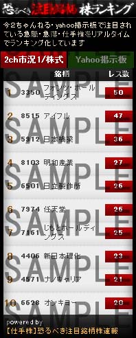
[3849]日本テクノ・ラボ 2ch&Yahoo板統合 新着口コミ情報
※コメントは常に更新されます
【急騰】今買えばいい株22245【全修】 より
17 :山師さん:2025/05/01(木)05:38:15 ID:ntL1FP6v
【速報】急騰・急落銘柄報告スレ18287 より
763 :山師さん@トレード中 :2025/05/01(木)03:10:48 ID:G1YqTSWC0
BREAKING: US reaches out to China recently for tariff discussions - Yuyuantantian.
速報:米国、関税協議のため中国に接触 - Yuyuantian.
やっぱりまだだったんだ(´・ω・`)
【急騰】今買えばいい株22232【GW雑談】 より
366 :山師さん:2025/04/27(日)21:15:15 ID:c+60HmU9
Recommended words to avoid
Captain
Kyoputen
Diarrhea
Tamaoji
Makibao
ZARD Man
Percy
Penirun
Pekora
Osakeski
Wisekey Man
Kirasura
Kirakira
Metaplaman
Spider
Babusura
Small fish
Gargle
Sniffed
Line break
Lost Money George
Other nicknames
Accounts that are deliberately involved with such pointless nicknames that are full of Virtua and Slime
It's a nuisance, so you guys should just start a separate thread and keep it private, most people aren't interested
【急騰】今買えばいい株22230【爆益ディスカ】 より
928 :山師さん:2025/04/26(土)03:03:43 ID:q3InTKVP
BREAKING: President Trump says another tariff pause is unlikely after the 90-day pause ends.
We are currently 16 days into the 90-day pause.
速報:トランプ大統領は、90日間の関税停止期間終了後に再度の関税停止が行われる可能性は低いと述べた。
現在、90 日間の休止期間の 16 日目が経過しています。
https://x.com/KobeissiLetter/status/1915828031865659576
【急騰】今買えばいい株22230【爆益ディスカ】 より
121 :山師さん:2025/04/25(金)18:18:02 ID:XRGCxQR+
Recommended words to avoid
Captain
Kyoputen
Diarrhea
Tamaoji
Makibao
ZARD Man
Percy
Penirun
Pekora
Osakeski
Wisekey Man
Kirasura
Kirakira
Metaplaman
Spider
Babusura
Small fish
Gargle
Sniffed
Line break
Lost Money George
Other nicknames
Accounts that are deliberately involved with such pointless nicknames that are full of Virtua and Slime
It's a nuisance, so you guys should just start a separate thread and keep it private, most people aren't interested
677 :山師さん:2025/04/25(金)21:37:18 lXSpXylc
>>121
今見てクソ吹いたわwwwwwww
261 :山師さん:2025/04/25(金)18:54:23 nbLg00zH
>>121
障害年金はどれに入るんだよ
179 :山師さん:2025/04/25(金)18:29:37 NyFcwCyn
>>121
おもろいな
150 :スパイダーM :2025/04/25(金)18:22:36 ++PVrW1R
>>121
改行がLinebreak(>ω<)
132 :たまおじ :2025/04/25(金)18:19:16 g7NoZq6I
>>121
ここも国際的なスレになったんだね☺
129 :山師さん:2025/04/25(金)18:19:03 fcCcfOn5
>>121
なんかかっこよくて草
128 :山師さん:2025/04/25(金)18:18:56 0fFRH4Y2
>>121
ワロタ
126 :山師さん:2025/04/25(金)18:18:51 Zlun9uTL
>>121
Linebreakで毎回笑う
122 :𓆜:2025/04/25(金)18:18:11 5Cot0BrH
>>121
草
【急騰】今買えばいい株22217【素チン】 より
189 :山師さん:2025/04/23(水)11:43:42 ID:upPe5xhk
Recommended words to avoid
Captain
Kyoputen
Diarrhea
Tamaoji
Makibao
ZARD Man
Percy
Penirun
Pekora
Osakeski
Wisekey Man
Kirasura
Kirakira
Metaplaman
Spider
Babusura
Small fish
Gargle
Sniffed
Line break
Lost Money George
Other nicknames
Accounts that are deliberately involved with such pointless nicknames that are full of Virtua and Slime
You're in the way, so just start a separate thread and keep it private, most people aren't interested
227 :山師さん:2025/04/23(水)11:52:39 14/JMGOQ
>>189
言われなくてもクソコテは昔から全員自動NGしとるしクソコテっぽいワードは全部NGワードぶち込んどるがな
221 :山師さん:2025/04/23(水)11:51:24 f19jOq8t
>>189
海外向けに日本の有名トレーダーアナウンスしないとな
213 :山師さん:2025/04/23(水)11:47:47 4RNCk79N
>>189
英語で書いてNGワード回避するの辞めろやゴミ
204 :山師さん:2025/04/23(水)11:46:16 sWWeDKms
>>189
障害年金はどれよ
203 :山師さん:2025/04/23(水)11:46:13 kWsk/Jjn
>>189
Linebreakでワロタ
198 :山師さん:2025/04/23(水)11:45:16 eVJoi+GV
>>189
外資機関投資家向けきたー
【急騰】今買えばいい株22213【修正】 より
656 :山師さん:2025/04/22(火)13:53:47 ID:4Dc97YHZ
Recommended words to avoid
Captain
Kyoputen
Diarrhea
Tamaoji
Makibao
ZARDman
Percy
Penirun
Pekora
Osakeski
Wisekeyman
Kirasura
Kirakira
Metaplaman
Spider
Babusura
Small fish
Gargle
Sniffed
Line break
Lost Money George
Other nicknames
Accounts that are deliberately involved with such pointless nicknames
It's annoying, so you guys should just start a separate thread and keep it private, most people aren't interested
660 :山師さん:2025/04/22(火)13:54:41 GG4eMcS7
>>656
クソコテっぽいワードは昔から全員NGワードにしてるわ俺は
658 :山師さん:2025/04/22(火)13:54:29 RHxXAXaG
>>656
しばきます
【急騰】今買えばいい株22208【団鬼六】 より
536 :山師さん:2025/04/21(月)22:53:54 ID:fbXSdLse
Amid Trump’s tariffs, TSMC has been stepping up its investment in the U.S. According to Economic Daily News, the company is accelerating the timeline for its second Arizona fab. In addition, TSMC is reportedly set to introduce its latest fan-out panel-level packaging (FOPLP) technology in the U.S. to meet rising demand from customers seeking chips manufactured in the U.S.
The report highlights that, following major clients such as Apple, NVIDIA, and AMD announcing plans to expand their investments in the U.S., TSMC has accordingly adjusted its strategies.
TSMC is currently in its quiet period ahead of its earnings call and is unable to comment, as the report notes.
TSMC Advances FOPLP Technology
Citing Nikkei, the report states that TSMC is finalizing the specifications for its FOPLP technology in an effort to accelerate its mass production timeline. The first-generation version is expected to adopt a 300mm x 300mm panel size—smaller than the previously tested 510mm x 515mm format. According to the report, TSMC is currently building a pilot production line in Taoyuan, Taiwan, with limited trial production anticipated to begin as early as 2027.
The report also notes that TSMC initially explored partnering with panel makers such as Innolux but ultimately opted to develop the technology in-house, as the current precision and technical capabilities of the panel industry were deemed insufficient to meet TSMC’s standards.
As noted by the report, FOPLP offers improved heat dissipation compared to 3D stacking techniques such as wafer-on-wafer (WoW), CoWoS, and SoIC. However, its production efficiency is lower than that of existing 3D stacking methods. The report adds that AI customers are still expected to be the primary adopters of this packaging technology.
Tech Giants Fuel TSMC’s U.S. Manufacturing Expansion
Notably, on April 15, AMD CEO Lisa Su confirmed that the company is ramping up U.S. production. According to Reuters, AMD’s flagship chips will soon roll off TSMC’s new Arizona line—marking the first time its products will be manufactured in the U.S.
Meanwhile, NVIDIA recently also revealed plans to invest up to USD 500 billion in U.S.-based AI server production over the next four years and confirmed that its Blackwell chips are now being produced at TSMC’s Phoenix plant, as Reuters notes.
As noted by Economic Daily News, sources indicate that in response to requests from major clients such as AMD and Apple, TSMC has reportedly informed suppliers that equipment move-in for its second Arizona fab will begin as early as September this year—one full year ahead of schedule.
In other words, the fab’s 3nm production is now expected to begin by the end of 2027, while the second-phase line for 2nm is projected to enter mass production in 2028 as the report points out.
547 :山師さん:2025/04/21(月)23:01:35 Rfp0DKa2
>>536
荒らすなボケ!
【急騰】今買えばいい株22208【団鬼六】 より
528 :山師さん:2025/04/21(月)22:51:37 ID:HQwTJw7C
Amid Trump’s tariffs, TSMC has been stepping up its investment in the U.S. According to Economic Daily News, the company is accelerating the timeline for its second Arizona fab. In addition, TSMC is reportedly set to introduce its latest fan-out panel-level packaging (FOPLP) technology in the U.S. to meet rising demand from customers seeking chips manufactured in the U.S.
The report highlights that, following major clients such as Apple, NVIDIA, and AMD announcing plans to expand their investments in the U.S., TSMC has accordingly adjusted its strategies.
TSMC is currently in its quiet period ahead of its earnings call and is unable to comment, as the report notes.
TSMC Advances FOPLP Technology
Citing Nikkei, the report states that TSMC is finalizing the specifications for its FOPLP technology in an effort to accelerate its mass production timeline. The first-generation version is expected to adopt a 300mm x 300mm panel size—smaller than the previously tested 510mm x 515mm format. According to the report, TSMC is currently building a pilot production line in Taoyuan, Taiwan, with limited trial production anticipated to begin as early as 2027.
The report also notes that TSMC initially explored partnering with panel makers such as Innolux but ultimately opted to develop the technology in-house, as the current precision and technical capabilities of the panel industry were deemed insufficient to meet TSMC’s standards.
As noted by the report, FOPLP offers improved heat dissipation compared to 3D stacking techniques such as wafer-on-wafer (WoW), CoWoS, and SoIC. However, its production efficiency is lower than that of existing 3D stacking methods. The report adds that AI customers are still expected to be the primary adopters of this packaging technology.
Tech Giants Fuel TSMC’s U.S. Manufacturing Expansion
Notably, on April 15, AMD CEO Lisa Su confirmed that the company is ramping up U.S. production. According to Reuters, AMD’s flagship chips will soon roll off TSMC’s new Arizona line—marking the first time its products will be manufactured in the U.S.
Meanwhile, NVIDIA recently also revealed plans to invest up to USD 500 billion in U.S.-based AI server production over the next four years and confirmed that its Blackwell chips are now being produced at TSMC’s Phoenix plant, as Reuters notes.
As noted by Economic Daily News, sources indicate that in response to requests from major clients such as AMD and Apple, TSMC has reportedly informed suppliers that equipment move-in for its second Arizona fab will begin as early as September this year—one full year ahead of schedule.
In other words, the fab’s 3nm production is now expected to begin by the end of 2027, while the second-phase line for 2nm is projected to enter mass production in 2028 as the report points out.
【急騰】今買えばいい株22208【団鬼六】 より
527 :山師さん:2025/04/21(月)22:51:14 ID:N5bUdpKO
Amid Trump’s tariffs, TSMC has been stepping up its investment in the U.S. According to Economic Daily News, the company is accelerating the timeline for its second Arizona fab. In addition, TSMC is reportedly set to introduce its latest fan-out panel-level packaging (FOPLP) technology in the U.S. to meet rising demand from customers seeking chips manufactured in the U.S.
The report highlights that, following major clients such as Apple, NVIDIA, and AMD announcing plans to expand their investments in the U.S., TSMC has accordingly adjusted its strategies.
TSMC is currently in its quiet period ahead of its earnings call and is unable to comment, as the report notes.
TSMC Advances FOPLP Technology
Citing Nikkei, the report states that TSMC is finalizing the specifications for its FOPLP technology in an effort to accelerate its mass production timeline. The first-generation version is expected to adopt a 300mm x 300mm panel size—smaller than the previously tested 510mm x 515mm format. According to the report, TSMC is currently building a pilot production line in Taoyuan, Taiwan, with limited trial production anticipated to begin as early as 2027.
The report also notes that TSMC initially explored partnering with panel makers such as Innolux but ultimately opted to develop the technology in-house, as the current precision and technical capabilities of the panel industry were deemed insufficient to meet TSMC’s standards.
As noted by the report, FOPLP offers improved heat dissipation compared to 3D stacking techniques such as wafer-on-wafer (WoW), CoWoS, and SoIC. However, its production efficiency is lower than that of existing 3D stacking methods. The report adds that AI customers are still expected to be the primary adopters of this packaging technology.
Tech Giants Fuel TSMC’s U.S. Manufacturing Expansion
Notably, on April 15, AMD CEO Lisa Su confirmed that the company is ramping up U.S. production. According to Reuters, AMD’s flagship chips will soon roll off TSMC’s new Arizona line—marking the first time its products will be manufactured in the U.S.
Meanwhile, NVIDIA recently also revealed plans to invest up to USD 500 billion in U.S.-based AI server production over the next four years and confirmed that its Blackwell chips are now being produced at TSMC’s Phoenix plant, as Reuters notes.
As noted by Economic Daily News, sources indicate that in response to requests from major clients such as AMD and Apple, TSMC has reportedly informed suppliers that equipment move-in for its second Arizona fab will begin as early as September this year—one full year ahead of schedule.
In other words, the fab’s 3nm production is now expected to begin by the end of 2027, while the second-phase line for 2nm is projected to enter mass production in 2028 as the report points out.
【急騰】今買えばいい株22208【団鬼六】 より
526 :山師さん:2025/04/21(月)22:51:03 ID:+p5wlGn+
Amid Trump’s tariffs, TSMC has been stepping up its investment in the U.S. According to Economic Daily News, the company is accelerating the timeline for its second Arizona fab. In addition, TSMC is reportedly set to introduce its latest fan-out panel-level packaging (FOPLP) technology in the U.S. to meet rising demand from customers seeking chips manufactured in the U.S.
The report highlights that, following major clients such as Apple, NVIDIA, and AMD announcing plans to expand their investments in the U.S., TSMC has accordingly adjusted its strategies.
TSMC is currently in its quiet period ahead of its earnings call and is unable to comment, as the report notes.
TSMC Advances FOPLP Technology
Citing Nikkei, the report states that TSMC is finalizing the specifications for its FOPLP technology in an effort to accelerate its mass production timeline. The first-generation version is expected to adopt a 300mm x 300mm panel size—smaller than the previously tested 510mm x 515mm format. According to the report, TSMC is currently building a pilot production line in Taoyuan, Taiwan, with limited trial production anticipated to begin as early as 2027.
The report also notes that TSMC initially explored partnering with panel makers such as Innolux but ultimately opted to develop the technology in-house, as the current precision and technical capabilities of the panel industry were deemed insufficient to meet TSMC’s standards.
As noted by the report, FOPLP offers improved heat dissipation compared to 3D stacking techniques such as wafer-on-wafer (WoW), CoWoS, and SoIC. However, its production efficiency is lower than that of existing 3D stacking methods. The report adds that AI customers are still expected to be the primary adopters of this packaging technology.
Tech Giants Fuel TSMC’s U.S. Manufacturing Expansion
Notably, on April 15, AMD CEO Lisa Su confirmed that the company is ramping up U.S. production. According to Reuters, AMD’s flagship chips will soon roll off TSMC’s new Arizona line—marking the first time its products will be manufactured in the U.S.
Meanwhile, NVIDIA recently also revealed plans to invest up to USD 500 billion in U.S.-based AI server production over the next four years and confirmed that its Blackwell chips are now being produced at TSMC’s Phoenix plant, as Reuters notes.
As noted by Economic Daily News, sources indicate that in response to requests from major clients such as AMD and Apple, TSMC has reportedly informed suppliers that equipment move-in for its second Arizona fab will begin as early as September this year—one full year ahead of schedule.
In other words, the fab’s 3nm production is now expected to begin by the end of 2027, while the second-phase line for 2nm is projected to enter mass production in 2028 as the report points out.
【急騰】今買えばいい株22208【団鬼六】 より
521 :山師さん:2025/04/21(月)22:50:11 ID:rwHZuuRz
Amid Trump’s tariffs, TSMC has been stepping up its investment in the U.S. According to Economic Daily News, the company is accelerating the timeline for its second Arizona fab. In addition, TSMC is reportedly set to introduce its latest fan-out panel-level packaging (FOPLP) technology in the U.S. to meet rising demand from customers seeking chips manufactured in the U.S.
The report highlights that, following major clients such as Apple, NVIDIA, and AMD announcing plans to expand their investments in the U.S., TSMC has accordingly adjusted its strategies.
TSMC is currently in its quiet period ahead of its earnings call and is unable to comment, as the report notes.
TSMC Advances FOPLP Technology
Citing Nikkei, the report states that TSMC is finalizing the specifications for its FOPLP technology in an effort to accelerate its mass production timeline. The first-generation version is expected to adopt a 300mm x 300mm panel size—smaller than the previously tested 510mm x 515mm format. According to the report, TSMC is currently building a pilot production line in Taoyuan, Taiwan, with limited trial production anticipated to begin as early as 2027.
The report also notes that TSMC initially explored partnering with panel makers such as Innolux but ultimately opted to develop the technology in-house, as the current precision and technical capabilities of the panel industry were deemed insufficient to meet TSMC’s standards.
As noted by the report, FOPLP offers improved heat dissipation compared to 3D stacking techniques such as wafer-on-wafer (WoW), CoWoS, and SoIC. However, its production efficiency is lower than that of existing 3D stacking methods. The report adds that AI customers are still expected to be the primary adopters of this packaging technology.
Tech Giants Fuel TSMC’s U.S. Manufacturing Expansion
Notably, on April 15, AMD CEO Lisa Su confirmed that the company is ramping up U.S. production. According to Reuters, AMD’s flagship chips will soon roll off TSMC’s new Arizona line—marking the first time its products will be manufactured in the U.S.
Meanwhile, NVIDIA recently also revealed plans to invest up to USD 500 billion in U.S.-based AI server production over the next four years and confirmed that its Blackwell chips are now being produced at TSMC’s Phoenix plant, as Reuters notes.
As noted by Economic Daily News, sources indicate that in response to requests from major clients such as AMD and Apple, TSMC has reportedly informed suppliers that equipment move-in for its second Arizona fab will begin as early as September this year—one full year ahead of schedule.
In other words, the fab’s 3nm production is now expected to begin by the end of 2027, while the second-phase line for 2nm is projected to enter mass production in 2028 as the report points out.
Yahoo掲示板(Y板) - 3849より
248 ::2025/04/19(土)08:54:00 ID: paypay
Yahoo掲示板(Y板) - 3849より
247 ::2025/04/18(金)17:58:00 ID:なよと
【急騰】今買えばいい株22191【Doする?手土産】 より
287 :山師さん:2025/04/16(水)21:48:23 ID:i93nKzV1
【速報】 米国、中国に245%の関税 中国以外の国の高関税は一時停止 ★3
https://asahi.5ch.net/test/read.cgi/newsplus/1744805008/1
1: お断り ★ 2025/04/16(水) 21:03:28.69 ID:8nf12XOb9
Today, President Donald J. Trump signed an Executive Order launching an investigation into the national security risks posed by U.S. reliance on imported processed critical minerals and their derivative products.
本日、トランプ大統領は米国が加工された重要鉱物とその派生製品の輸入に依存していることがもたらす国家安全保障上のリスクについて調査開始する大統領令に署名を行った。
As a result, the individualized higher tariffs are currently paused amid these discussions, except for China, which retaliated.
報復措置を取った中国を除き、個別の高関税の導入は協議が続く中で現在一時停止している。
China now faces up to a 245% tariff on imports to the United States as a result of its retaliatory actions.
中国は報復措置の結果、米国への輸入品に最大245%の関税を課す。
ホワイトハウス公式 (現地時間)2025/4/15 ソース英語『Fact Sheet: President Donald J. Trump Ensures National Security and Economic Resilience Through Section 232 Actions on Processed Critical Minerals and Derivative Products』
https://www.whitehouse.gov/fact-sheets/2025/04/fact-sheet-president-donald-j-trump-ensures-national-security-and-economic-resilience-through-section-232-actions-on-processed-critical-minerals-and-derivative-products/
【急騰】今買えばいい株22156【世界変革の時】 より
788 :山師さん:2025/04/10(木)00:20:19 ID:R7wYE3t+
SCOOP: People close to the Trump White House say you can expect an announcement of some sort about formal negotiations over trade and tariffs with Japan, Vietnam, and possibly the UK as early as today. Im not sure how much this moves the needle if it does go down (I always hedge w Trump who is unpredictable and these are inherently unpredictable times). Japan and Vietnam were already moving in this direction; UK is a long-time trading partner. But it's better than the alternative. And it does change the market narrative of doom and gloom. Story developing
790 :山師さん:2025/04/10(木)00:20:41 XiYsJ6UZ
>>788
キタ━━━━(゚∀゚)━━━━!!
Yahoo掲示板(Y板) - 3849より
246 :>このような対…:2025/03/27(木)16:33:00 ID:大人株主観***********
> このような対応は、株主や投資家に対する配慮が不足していると受け取られ、企業の信頼を損なう可能性があります。 日本テクノラボが配当を発表した翌日に最安値を更新し、自社株買いを実施したにも関わらず最安値を更新したという状況は、投資家の信頼を回復するのが非常に難しい状況であることを示唆していると考えられます。 一般的に、配当の実施や自社株買いは株主還元策とみなされ、株価の押し上げ要因となることが多いです。しかし、今回のケースでは、これらの施策が市場にポジティブに受け止められなかったということになります。 過去に投資家を失望させるような出来事があった場合、一度失われた信頼を取り戻すには、時間と具体的な実績が必要になります。今回の配当や自社株買いだけでは、過去のネガティブなイメージを払拭できなかった可能性があります。
Yahoo掲示板(Y板) - 3849より
245 :配当発表タイミングに…:2025/03/27(木)16:27:00 ID:大人株主観***********
配当発表タイミングについて、2025年3月25日の取引終了後の発表で、基準日が2025年3月31日というのは、投資家にとってたった2日間しか取引期間がありません。 取引期間が非常に短く、混乱を招く可能性がありますね。 通常、期末配当の権利を得るための最終売買日は、権利確定日の2営業日前となりますので、つまり、2025年3月末の権利付最終売買日は3月27日(木)、権利落ち日は3月28日(金)、権利確定日は3月31日(月)となります。 今回の発表は、権利付最終売買日の2営業日前の取引時間終了後に行われたため、実際にこの配当を得るためには、 3月26日(水)と 3月27日(木)の2日間しか取引期間がありません。 このような対応は、株主や投資家に対する配慮が不足していると受け取られ、企業の信頼を損なう可能性があります。 上場企業には、株主や投資家に対して適切な情報開示を適切なタイミングで行う責任があります。今回の日本テクノ・ラボの発表タイミングは、その点で問題があったと言えるでしょう。 今後の情報開示においては、投資家が十分な時間を持って判断できるよう、より早期の発表を期待したいところです。
Yahoo掲示板(Y板) - 3849より
244 :配当発表時期について…:2025/03/27(木)16:24:00 ID:大人株主観***********
配当発表時期について、2025年3月25日の取引終了後の発表で、基準日が2025年3月31日というのは、投資家にとってたった2日間しか取引期間がありません。 取引期間が非常に短く、混乱を招く可能性がありますね。 通常、期末配当の権利を得るための最終売買日は、権利確定日の2営業日前となりますので、つまり、2025年3月末の権利付最終売買日は3月27日(木)、権利落ち日は3月28日(金)、権利確定日は3月31日(月)となります。 今回の発表は、権利付最終売買日の2営業日前の取引時間終了後に行われたため、実際にこの配当を得るためには、 3月26日(水)と 3月27日(木)の2日間しか取引期間がありません。 このような対応は、株主や投資家に対する配慮が不足していると受け取られ、企業の信頼を損なう可能性があります。 上場企業には、株主や投資家に対して適切な情報開示を適切なタイミングで行う責任があります。今回の日本テクノ・ラボの発表タイミングは、その点で問題があったと言えるでしょう。 今後の情報開示においては、投資家が十分な時間を持って判断できるよう、より早期の発表を期待したいところです。
Yahoo掲示板(Y板) - 3849より
243 :現状を踏まえると、:2025/03/25(火)18:38:00 ID:大人株主観***********
現状を踏まえると、ナルテックの破産による技術的な悪影響は、今後も尾を引く可能性が高いと考えられます。 また、権利落ち日以降は、配当の10円を大きく超える株価の下落も想定しておく必要があるでしょう。 > 落ち日以降、株価はさらに下がる可能性が高いでしょう。
Yahoo掲示板(Y板) - 3849より
242 : 現状を踏まえると、…:2025/03/25(火)18:07:00 ID:大人株主観***********
現状を踏まえると、ナルテックの破産による技術的な悪影響は、今後も尾を引く可能性が高いと考えられます。 また、権利落ち日以降は、配当の10円を大きく超える株価の下落も想定しておく必要があるでしょう。 > 落ち日以降、株価はさらに下がる可能性が高いでしょう。
Yahoo掲示板(Y板) - 3849より
241 :今日も安値更新とは、…:2025/03/21(金)17:36:00 ID:大人株主観***********
今日も安値更新とは、厳しいですね。 落ち日以降、株価はさらに下がる可能性が高いでしょう。 今のままではナルテックの破産による技術的な影響は今後も続くでしょう。 しかし、株価が下がれば下がるほど、その会社の価値は高まると信じて、今後の展開に期待しましょう。 > 株価が下がるほど、価値が上がる会社であり、、、期待する。
Yahoo掲示板(Y板) - 3849より
240 :>株価が下がる…:2025/03/20(木)14:56:00 ID:大人株主観***********
> 株価が下がるほど、価値が上がる会社であり、、、期待する。 ゆうこりんさんの考え方は斬新的ですね。 「会社の価値を上げるために、 もっと株価を下げた方がいい。 そうすれば社長と仲良くなれる」 ということでしょうか。 株価を下げることが会社の価値を上げることにつながるという考え方は一般的ではないため、その背景や意図をより分かりやすく説明していただけますでしょうか。 あ、ホヤ貝 旬の
Yahoo掲示板(Y板) - 3849より
238 :大根の恨みつらみは、…:2025/03/19(水)21:55:00 ID:ゆうこりん
大根の恨みつらみは、さておいて、この規模ならば、悪い年も良い年もあるという現実。 嫌なら株を持たなければ良い。 好きなら買い増せば良い。 そこに制約も、縛りもない。 村上ファンドのように、モノ言う株主気取りならば、この会社でやらずに、もっと大きい株式会社でやってみれば良い。 社長への恨みで、ここに書き込む奴は、鏡をみれば良い。 株価が下がるほど、価値が上がる会社であり、そこからの伸び上がりを期待する。
続きは3849銘柄情報ページでご確認ください
掲示板書き込み
- スパム対策の為、URLは"h"を抜いた"ttp"から入力して下さい。
- 宣伝目的と思われる書き込みに記載されたURLにはサイト内銘柄ページ、ブログランキング他、当サイトからのリンクを全て除外させて頂きます。
銘柄別掲示板一覧
- 【3475】 グッドコムアセット(1)
- 【9468】 KADOKAWA(1)
- 【2120】 LIFULL(1)
- 【6743】 大同信号(5)
- 【2330】 フォーサイド(1)
- 【6301】 コマツ(2)
- 【3686】 ディー・エル・イー(1)
- 【2767】 円谷フィールズホールディングス(1)
- 【3399】 丸千代山岡家(1)
- 【3133】 海帆(1)
- 【8226】 理経(5)
- 【6966】 三井ハイテック(1)
- 【9504】 中国電力(1)
- 【2764】 ひらまつ(37)
- 【9558】 ジャパニアス(1)
- 【2370】 メディネット(10)
- 【3401】 帝人(3)
- 【2418】 ツカダ・グローバルホールディング(1)
- 【2157】 コシダカホールディングス(1)
- 【3099】 三越伊勢丹ホールディングス(1)
- 【8233】 高島屋(1)
- 【6191】 エアトリ(1)
- 【7554】 幸楽苑(1)
- 【3030】 ハブ(1)
- 【3481】 三菱地所物流リート投資法人(1)
- 【3907】 シリコンスタジオ(20)
- 【3470】 マリモ地方創生リート投資法人(1)
- 【6753】 シャープ(9)
- 【2698】 キャンドゥ(1)
- 【3940】 ノムラシステムコーポレーション(1)
912:山師さん:[sage]:2025/05/01(木) 00:11:28.35 ID:ntL1FP6v
朝には+300くらいか?
売り豚可哀想😢
当たった😂