7646(株)PLANT
市場:東証STD
業種:小売業
Plant Co。、Ltd。主にディスカウントストアの運営に関与している会社です。同社は、Joyful Store、Home Center、Super Centerという名前で3種類の店舗を運営しています。 Joyful Storeは都市部にあり、主に小型および小規模の食料品やその他の毎日の消耗品を提供しています。ホームセンターは郊外にあり、主に自分自身(DIY)アイテム、庭用品、生鮮食品を除く食品、衣類を供給しています。スーパーセンターは農村部にあり、主に生鮮食品などを含む日常の生活関連製品を提供しています。
関連: ディスカウント/生活防衛/日用品/あえてスタンダード
スポンサード リンク
スポンサード リンク
- 全て表示
- 関連ブログ情報
- 【2ch】市況1/株式板(5ch)
- 【Yahoo】ファイナンス掲示板
- twitter呟き
- [7646]PLANT 株式掲示板
関連ブログ情報 新着リスト
-
-
2025/04/30 PR PLANT(7646)を今から買って大丈夫か?不安要素はいくつかあります…。
- 株式投資の世界で勝ち続けるためには、「銘柄の選定」と「銘柄の売買タイミング」が大事です。適当な銘柄選定では勝てませんし、売買タイミングを誤ってしまうと…
- https://exiv.ne.jp/
-
-
-
2024/12/19 大雪の到着優待。(6)
- 本日の到着優待は八洲電機(3153)のジェフグルメカードと、PLANT(7646)のPLANTpay1000円分。PLANTpayは同封されている書類の中に株主専用web販売サイトのURLがあり、そちらでカードの裏面に書かれたIDを入力すると無料で商品が購入できるので、実質選べるギフトと同じ内容
- http://blog.livedoor.jp/ks_kabunon/archives/53074706.html
-
-
-
2024/11/21 2024-11-21(木)の高配当 良チャートメモ
- ※スクリーニング結果のメモであり、投資を推奨するものではありません。※投資は自己責任で\(^o^)/ 高配当 良チャートメモ 【256A】飛島ホールディングス(利回り5.68%)【9101】日本郵船(利回り5.16%)【7646】PLANT
- https://eagle-trade.sytes.net/archives/1745
-
-
-
2024/11/21 PLANT(7646)の株主還元と事業リスク
- PLANT(7646)は1982年に「株式会社みった」として家庭用品やプロパンガス専門店として創業を開始しています。現在のスーパーセンターPLANTの初出店は1990年11月に福井県鯖江市でのオープンとなり、2024年11月19日時点では13県に23店舗を展開しています。出所:PLANT 2024
- https://gazoo.work/archives/37275148.html
-
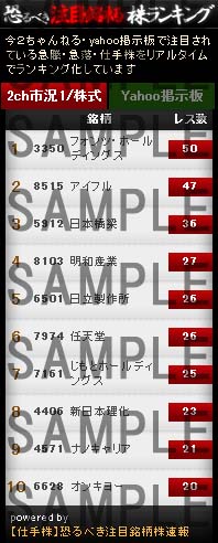
【2ch】市況1板、株式板の反応(新着順)
スポンサード リンク
【急騰】今買えばいい株22241【石破減配祭り】 より
366 :山師さん:2025/04/30(水)13:19:22 ID:oolPhORB.net
【急騰】今買えばいい株22208【団鬼六】 より
536 :山師さん:2025/04/21(月)22:53:54 ID:fbXSdLse.net
Amid Trump’s tariffs, TSMC has been stepping up its investment in the U.S. According to Economic Daily News, the company is accelerating the timeline for its second Arizona fab. In addition, TSMC is reportedly set to introduce its latest fan-out panel-level packaging (FOPLP) technology in the U.S. to meet rising demand from customers seeking chips manufactured in the U.S.
The report highlights that, following major clients such as Apple, NVIDIA, and AMD announcing plans to expand their investments in the U.S., TSMC has accordingly adjusted its strategies.
TSMC is currently in its quiet period ahead of its earnings call and is unable to comment, as the report notes.
TSMC Advances FOPLP Technology
Citing Nikkei, the report states that TSMC is finalizing the specifications for its FOPLP technology in an effort to accelerate its mass production timeline. The first-generation version is expected to adopt a 300mm x 300mm panel size—smaller than the previously tested 510mm x 515mm format. According to the report, TSMC is currently building a pilot production line in Taoyuan, Taiwan, with limited trial production anticipated to begin as early as 2027.
The report also notes that TSMC initially explored partnering with panel makers such as Innolux but ultimately opted to develop the technology in-house, as the current precision and technical capabilities of the panel industry were deemed insufficient to meet TSMC’s standards.
As noted by the report, FOPLP offers improved heat dissipation compared to 3D stacking techniques such as wafer-on-wafer (WoW), CoWoS, and SoIC. However, its production efficiency is lower than that of existing 3D stacking methods. The report adds that AI customers are still expected to be the primary adopters of this packaging technology.
Tech Giants Fuel TSMC’s U.S. Manufacturing Expansion
Notably, on April 15, AMD CEO Lisa Su confirmed that the company is ramping up U.S. production. According to Reuters, AMD’s flagship chips will soon roll off TSMC’s new Arizona line—marking the first time its products will be manufactured in the U.S.
Meanwhile, NVIDIA recently also revealed plans to invest up to USD 500 billion in U.S.-based AI server production over the next four years and confirmed that its Blackwell chips are now being produced at TSMC’s Phoenix plant, as Reuters notes.
As noted by Economic Daily News, sources indicate that in response to requests from major clients such as AMD and Apple, TSMC has reportedly informed suppliers that equipment move-in for its second Arizona fab will begin as early as September this year—one full year ahead of schedule.
In other words, the fab’s 3nm production is now expected to begin by the end of 2027, while the second-phase line for 2nm is projected to enter mass production in 2028 as the report points out.
【急騰】今買えばいい株22208【団鬼六】 より
528 :山師さん:2025/04/21(月)22:51:37 ID:HQwTJw7C.net
Amid Trump’s tariffs, TSMC has been stepping up its investment in the U.S. According to Economic Daily News, the company is accelerating the timeline for its second Arizona fab. In addition, TSMC is reportedly set to introduce its latest fan-out panel-level packaging (FOPLP) technology in the U.S. to meet rising demand from customers seeking chips manufactured in the U.S.
The report highlights that, following major clients such as Apple, NVIDIA, and AMD announcing plans to expand their investments in the U.S., TSMC has accordingly adjusted its strategies.
TSMC is currently in its quiet period ahead of its earnings call and is unable to comment, as the report notes.
TSMC Advances FOPLP Technology
Citing Nikkei, the report states that TSMC is finalizing the specifications for its FOPLP technology in an effort to accelerate its mass production timeline. The first-generation version is expected to adopt a 300mm x 300mm panel size—smaller than the previously tested 510mm x 515mm format. According to the report, TSMC is currently building a pilot production line in Taoyuan, Taiwan, with limited trial production anticipated to begin as early as 2027.
The report also notes that TSMC initially explored partnering with panel makers such as Innolux but ultimately opted to develop the technology in-house, as the current precision and technical capabilities of the panel industry were deemed insufficient to meet TSMC’s standards.
As noted by the report, FOPLP offers improved heat dissipation compared to 3D stacking techniques such as wafer-on-wafer (WoW), CoWoS, and SoIC. However, its production efficiency is lower than that of existing 3D stacking methods. The report adds that AI customers are still expected to be the primary adopters of this packaging technology.
Tech Giants Fuel TSMC’s U.S. Manufacturing Expansion
Notably, on April 15, AMD CEO Lisa Su confirmed that the company is ramping up U.S. production. According to Reuters, AMD’s flagship chips will soon roll off TSMC’s new Arizona line—marking the first time its products will be manufactured in the U.S.
Meanwhile, NVIDIA recently also revealed plans to invest up to USD 500 billion in U.S.-based AI server production over the next four years and confirmed that its Blackwell chips are now being produced at TSMC’s Phoenix plant, as Reuters notes.
As noted by Economic Daily News, sources indicate that in response to requests from major clients such as AMD and Apple, TSMC has reportedly informed suppliers that equipment move-in for its second Arizona fab will begin as early as September this year—one full year ahead of schedule.
In other words, the fab’s 3nm production is now expected to begin by the end of 2027, while the second-phase line for 2nm is projected to enter mass production in 2028 as the report points out.
【急騰】今買えばいい株22208【団鬼六】 より
527 :山師さん:2025/04/21(月)22:51:14 ID:N5bUdpKO.net
Amid Trump’s tariffs, TSMC has been stepping up its investment in the U.S. According to Economic Daily News, the company is accelerating the timeline for its second Arizona fab. In addition, TSMC is reportedly set to introduce its latest fan-out panel-level packaging (FOPLP) technology in the U.S. to meet rising demand from customers seeking chips manufactured in the U.S.
The report highlights that, following major clients such as Apple, NVIDIA, and AMD announcing plans to expand their investments in the U.S., TSMC has accordingly adjusted its strategies.
TSMC is currently in its quiet period ahead of its earnings call and is unable to comment, as the report notes.
TSMC Advances FOPLP Technology
Citing Nikkei, the report states that TSMC is finalizing the specifications for its FOPLP technology in an effort to accelerate its mass production timeline. The first-generation version is expected to adopt a 300mm x 300mm panel size—smaller than the previously tested 510mm x 515mm format. According to the report, TSMC is currently building a pilot production line in Taoyuan, Taiwan, with limited trial production anticipated to begin as early as 2027.
The report also notes that TSMC initially explored partnering with panel makers such as Innolux but ultimately opted to develop the technology in-house, as the current precision and technical capabilities of the panel industry were deemed insufficient to meet TSMC’s standards.
As noted by the report, FOPLP offers improved heat dissipation compared to 3D stacking techniques such as wafer-on-wafer (WoW), CoWoS, and SoIC. However, its production efficiency is lower than that of existing 3D stacking methods. The report adds that AI customers are still expected to be the primary adopters of this packaging technology.
Tech Giants Fuel TSMC’s U.S. Manufacturing Expansion
Notably, on April 15, AMD CEO Lisa Su confirmed that the company is ramping up U.S. production. According to Reuters, AMD’s flagship chips will soon roll off TSMC’s new Arizona line—marking the first time its products will be manufactured in the U.S.
Meanwhile, NVIDIA recently also revealed plans to invest up to USD 500 billion in U.S.-based AI server production over the next four years and confirmed that its Blackwell chips are now being produced at TSMC’s Phoenix plant, as Reuters notes.
As noted by Economic Daily News, sources indicate that in response to requests from major clients such as AMD and Apple, TSMC has reportedly informed suppliers that equipment move-in for its second Arizona fab will begin as early as September this year—one full year ahead of schedule.
In other words, the fab’s 3nm production is now expected to begin by the end of 2027, while the second-phase line for 2nm is projected to enter mass production in 2028 as the report points out.
【急騰】今買えばいい株22208【団鬼六】 より
526 :山師さん:2025/04/21(月)22:51:03 ID:+p5wlGn+.net
Amid Trump’s tariffs, TSMC has been stepping up its investment in the U.S. According to Economic Daily News, the company is accelerating the timeline for its second Arizona fab. In addition, TSMC is reportedly set to introduce its latest fan-out panel-level packaging (FOPLP) technology in the U.S. to meet rising demand from customers seeking chips manufactured in the U.S.
The report highlights that, following major clients such as Apple, NVIDIA, and AMD announcing plans to expand their investments in the U.S., TSMC has accordingly adjusted its strategies.
TSMC is currently in its quiet period ahead of its earnings call and is unable to comment, as the report notes.
TSMC Advances FOPLP Technology
Citing Nikkei, the report states that TSMC is finalizing the specifications for its FOPLP technology in an effort to accelerate its mass production timeline. The first-generation version is expected to adopt a 300mm x 300mm panel size—smaller than the previously tested 510mm x 515mm format. According to the report, TSMC is currently building a pilot production line in Taoyuan, Taiwan, with limited trial production anticipated to begin as early as 2027.
The report also notes that TSMC initially explored partnering with panel makers such as Innolux but ultimately opted to develop the technology in-house, as the current precision and technical capabilities of the panel industry were deemed insufficient to meet TSMC’s standards.
As noted by the report, FOPLP offers improved heat dissipation compared to 3D stacking techniques such as wafer-on-wafer (WoW), CoWoS, and SoIC. However, its production efficiency is lower than that of existing 3D stacking methods. The report adds that AI customers are still expected to be the primary adopters of this packaging technology.
Tech Giants Fuel TSMC’s U.S. Manufacturing Expansion
Notably, on April 15, AMD CEO Lisa Su confirmed that the company is ramping up U.S. production. According to Reuters, AMD’s flagship chips will soon roll off TSMC’s new Arizona line—marking the first time its products will be manufactured in the U.S.
Meanwhile, NVIDIA recently also revealed plans to invest up to USD 500 billion in U.S.-based AI server production over the next four years and confirmed that its Blackwell chips are now being produced at TSMC’s Phoenix plant, as Reuters notes.
As noted by Economic Daily News, sources indicate that in response to requests from major clients such as AMD and Apple, TSMC has reportedly informed suppliers that equipment move-in for its second Arizona fab will begin as early as September this year—one full year ahead of schedule.
In other words, the fab’s 3nm production is now expected to begin by the end of 2027, while the second-phase line for 2nm is projected to enter mass production in 2028 as the report points out.
【急騰】今買えばいい株22208【団鬼六】 より
521 :山師さん:2025/04/21(月)22:50:11 ID:rwHZuuRz.net
Amid Trump’s tariffs, TSMC has been stepping up its investment in the U.S. According to Economic Daily News, the company is accelerating the timeline for its second Arizona fab. In addition, TSMC is reportedly set to introduce its latest fan-out panel-level packaging (FOPLP) technology in the U.S. to meet rising demand from customers seeking chips manufactured in the U.S.
The report highlights that, following major clients such as Apple, NVIDIA, and AMD announcing plans to expand their investments in the U.S., TSMC has accordingly adjusted its strategies.
TSMC is currently in its quiet period ahead of its earnings call and is unable to comment, as the report notes.
TSMC Advances FOPLP Technology
Citing Nikkei, the report states that TSMC is finalizing the specifications for its FOPLP technology in an effort to accelerate its mass production timeline. The first-generation version is expected to adopt a 300mm x 300mm panel size—smaller than the previously tested 510mm x 515mm format. According to the report, TSMC is currently building a pilot production line in Taoyuan, Taiwan, with limited trial production anticipated to begin as early as 2027.
The report also notes that TSMC initially explored partnering with panel makers such as Innolux but ultimately opted to develop the technology in-house, as the current precision and technical capabilities of the panel industry were deemed insufficient to meet TSMC’s standards.
As noted by the report, FOPLP offers improved heat dissipation compared to 3D stacking techniques such as wafer-on-wafer (WoW), CoWoS, and SoIC. However, its production efficiency is lower than that of existing 3D stacking methods. The report adds that AI customers are still expected to be the primary adopters of this packaging technology.
Tech Giants Fuel TSMC’s U.S. Manufacturing Expansion
Notably, on April 15, AMD CEO Lisa Su confirmed that the company is ramping up U.S. production. According to Reuters, AMD’s flagship chips will soon roll off TSMC’s new Arizona line—marking the first time its products will be manufactured in the U.S.
Meanwhile, NVIDIA recently also revealed plans to invest up to USD 500 billion in U.S.-based AI server production over the next four years and confirmed that its Blackwell chips are now being produced at TSMC’s Phoenix plant, as Reuters notes.
As noted by Economic Daily News, sources indicate that in response to requests from major clients such as AMD and Apple, TSMC has reportedly informed suppliers that equipment move-in for its second Arizona fab will begin as early as September this year—one full year ahead of schedule.
In other words, the fab’s 3nm production is now expected to begin by the end of 2027, while the second-phase line for 2nm is projected to enter mass production in 2028 as the report points out.
【速報】急騰・急落銘柄報告スレ18253 より
909 :山師さん@トレード中 :2025/04/15(火)15:46:26 ID:vLjn/z0F0.net
US chipmakers outsourcing manufacturing will escape China's tariffs(ロイター)
製造委託する米チップメーカーは中国の関税から逃れられるか
記事内
「"For all integrated circuits, whether packaged or unpackaged, the declared country of origin
for import customs purchases is the location of the wafer fabrication plant," 」
「包装されたすべての統合サーキットについては、包装されているか、梱包されていないかにかかわらず、
輸入税関の購入のために宣言された原産国は、ウェーハ製造工場の場所です。」
3日前の記事だけど、こう言う関税回避の手段って、トランプ政権内に睨まれているんだろうな (´・ω・`)
【速報】急騰・急落銘柄報告スレ18251 より
332 :山師さん@トレード中:2025/04/14(月)22:17:25 ID:rkpB0GSn0.net
NVIDIA Blackwell chips have started production at TSMC's chip plants in Phoenix, Arizona.
エヌビディア・ブラックウェル・チップは、アリゾナ州フェニックスにあるTSMCのチップ工場で生産を開始した。
だそうです(´・ω・`)
板別にレスを表示する
Yahoo掲示板(Y板)の反応(新着順)
スポンサード リンク
2025/04/30(水) 18:22:00投稿者:e9e*****
今日の大口の買いはなんでしょうね?
期待しかないですね!
2025/04/30(水) 16:20:00投稿者:ユニコーン
おっ1500が見えてきましたね。
2025/04/30(水) 13:38:00投稿者:ユニコーン
何この動き?
口座乗っ取りでも起きたか?
2025/04/30(水) 13:00:00投稿者:ユニコーン
はい、含み益転換
今回のトランプショックで600株だけですが買い増し致しました。
2025/04/28(月) 17:47:00投稿者:ユニコーン
今日は全く見てなかったけど後場は特売りスタート?
でオークションも大安売り?
2025/04/28(月) 11:40:00投稿者:ユニコーン
としかして減配懸念されてたのか?現物で安く手放した人はドンマイ。
現物最強だね
2025/04/28(月) 09:43:00投稿者:かまん
無事通過
2025/04/25(金) 21:43:00投稿者:暴れん棒将軍
高配当維持だけで十分
2025/04/25(金) 16:28:00投稿者:かまん
決算
2025/04/25(金) 11:37:00投稿者:ユニコーン
まぁもう2Qの業績は発表されたようなもんやし明らかな高配当株で信用買いもすくないから安心して買える希少銘柄だと思うけどな。
3年持ち続けたらまず負けはないと思う。
twitter検索
![]() |
kabudev_gc
2023年07月07日 (金) 週足 25週↑200週移動平均線
4707 キタック
4381 ビープラッツ
7229 ユタカ技研
3733 ソフトウェア・サービス
6297 鉱研工業
7259 アイシン
7646 PLANT… https://t.co/Uc1PWPk6rL |
---|
7646特売り