shinseijapan

【恐るべき株】今急騰/急落している株、仕手株、低位株、思惑株、材料株など、今みんなが注目している銘柄をほぼリアルタイムでランキング化!個別株銘柄情報も口コミや掲示板など中心にまとめています。
【2ch】急騰株 急落株 仕手株 注目銘柄【Yahoo】ファイナンス掲示板(Y板)よりそれぞれの注目銘柄ランキングが表示され、 レス数ボタン・トピ数ボタンをクリックする事で最新銘柄口コミ情報が表示されます!気になる株式銘柄がある方は是非お試しください。 仕手・仕手株・仕手筋とは?

[お知らせ]
リアルタイム注目キーワードランキング をホームに設置しました。2ch市況1/株式板で今リアルタイムで話題の注目キーワードをご覧ください。 ※現在1位のキーワードは『オルツ』です
本日、仕手株として話題になっている銘柄は 仕手・仕手株 こちらの検索結果をご参考に。

【4631】DIC【4631】

1 : 管理人 : 2012/07/30(月) 20:32:49 ID:OwnerKabu685

DIC[4631] - 国内インキ2位、米欧インキ会社サンケミカルを傘下に収め世界市場は首位。インキ以外は樹脂を中心とした工業材料事業、プラスチック成型品等の機能製品事業、電子情報材料事業など多彩な展開。インキのアジア、東欧での需要取り込みや、工業材料の中国での販売拡大、液晶等の次世代製品・事業の早期戦略化に注力。欧米の工業材料事業子会社を売却するなどリストラを進める一方、インキの世界最適生産体制構築など再編を積極推進。

会社HP:ttp://www.dic-global.com/

前へ次へ

現在書き込みはありません。
DICを保有している方や思惑のある方は、ぜひ書き込みして行ってください!

DICの銘柄情報はコチラ→4631

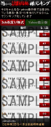
[4631]DIC 2ch&Yahoo板統合 新着口コミ情報

※コメントは常に更新されます

Yahoo掲示板(Y板) - 4631より

495 :BtoBの企業で、:2025/05/01(木)10:37:00 ID:san*****

BtoBの企業で、一般個人に知名度がないからこそ、個人向けの優待カレンダーくらいは残すべきだと私も思っていました。 使っているインキは自社製品なんだからPRにもなるし。 美術館縮小の件といい、がっかりではあります。 ま、資本効率を高めろという株主もいるわけで、株価上昇に期待(そうしたら売却する予定)していますが、 今のところそっちの方もサッパリだめでは、踏んだり蹴ったり。

Yahoo掲示板(Y板) - 4631より

494 ::2025/04/30(水)21:59:00 ID:old*****

太陽ホールディングスさん買ってください

Yahoo掲示板(Y板) - 4631より

493 :毎年、:2025/04/30(水)15:32:00 ID:ちょうきんぺい

毎年、オークションに500円くらいで出品されてましたね 価格相応。。な株主優待

Yahoo掲示板(Y板) - 4631より

492 :カレンダーだけは残し…:2025/04/30(水)14:53:00 ID:4ad*****

カレンダーだけは残して欲しいと願う株主です。 色・センス良く、さすがインキ屋さんと、毎年楽しみにしていたのに…

Yahoo掲示板(Y板) - 4631より

491 :ほんと、:2025/04/30(水)13:22:00 ID:マック ドナルド

ほんと、ファンドの買い増しか?

Yahoo掲示板(Y板) - 4631より

490 :どうした:2025/04/30(水)13:21:00 ID:has*****

どうした

Yahoo掲示板(Y板) - 4631より

489 :後ろめたいことあるか…:2025/04/29(火)15:16:00 ID:チキン虎ヌ狸

後ろめたいことあるからさっさと美術館始末するので。目くらまし。オーナーさんの会社との取引が不透明に思えるます。定款変更可決されたらよかった

Yahoo掲示板(Y板) - 4631より

488 :本社ビルの賃料を創業…:2025/04/28(月)14:59:00 ID:slc*****

本社ビルの賃料を創業家が得ている構図なのね。こういう会社の私物化はだめだね。問題視した香港ファンド頑張ってほしい

Yahoo掲示板(Y板) - 4631より

487 :1.コオロギは風説の…:2025/04/24(木)17:42:00 ID:放置民

1.コオロギは風説の流布とかじゃなかったっけ。会社は潰されちゃった! 2.株主資本を文化価値創出メインにするのは本末転倒でしょ。

Yahoo掲示板(Y板) - 4631より

486 :配当安定って、:2025/04/23(水)20:21:00 ID:old*****

配当安定って、減配か横ばいしかしてないのですが、、、

Yahoo掲示板(Y板) - 4631より

485 :何が言いたいのか判ら…:2025/04/23(水)17:25:00 ID:ちょうきんぺい

何が言いたいのか判らない、ただの美術愛好家か

【急騰】今買えばいい株22208【団鬼六】 より

536 :山師さん:2025/04/21(月)22:53:54 ID:fbXSdLse

Amid Trump’s tariffs, TSMC has been stepping up its investment in the U.S. According to Economic Daily News, the company is accelerating the timeline for its second Arizona fab. In addition, TSMC is reportedly set to introduce its latest fan-out panel-level packaging (FOPLP) technology in the U.S. to meet rising demand from customers seeking chips manufactured in the U.S.

The report highlights that, following major clients such as Apple, NVIDIA, and AMD announcing plans to expand their investments in the U.S., TSMC has accordingly adjusted its strategies.

TSMC is currently in its quiet period ahead of its earnings call and is unable to comment, as the report notes.

TSMC Advances FOPLP Technology

Citing Nikkei, the report states that TSMC is finalizing the specifications for its FOPLP technology in an effort to accelerate its mass production timeline. The first-generation version is expected to adopt a 300mm x 300mm panel size—smaller than the previously tested 510mm x 515mm format. According to the report, TSMC is currently building a pilot production line in Taoyuan, Taiwan, with limited trial production anticipated to begin as early as 2027.

The report also notes that TSMC initially explored partnering with panel makers such as Innolux but ultimately opted to develop the technology in-house, as the current precision and technical capabilities of the panel industry were deemed insufficient to meet TSMC’s standards.

As noted by the report, FOPLP offers improved heat dissipation compared to 3D stacking techniques such as wafer-on-wafer (WoW), CoWoS, and SoIC. However, its production efficiency is lower than that of existing 3D stacking methods. The report adds that AI customers are still expected to be the primary adopters of this packaging technology.

Tech Giants Fuel TSMC’s U.S. Manufacturing Expansion

Notably, on April 15, AMD CEO Lisa Su confirmed that the company is ramping up U.S. production. According to Reuters, AMD’s flagship chips will soon roll off TSMC’s new Arizona line—marking the first time its products will be manufactured in the U.S.

Meanwhile, NVIDIA recently also revealed plans to invest up to USD 500 billion in U.S.-based AI server production over the next four years and confirmed that its Blackwell chips are now being produced at TSMC’s Phoenix plant, as Reuters notes.

As noted by Economic Daily News, sources indicate that in response to requests from major clients such as AMD and Apple, TSMC has reportedly informed suppliers that equipment move-in for its second Arizona fab will begin as early as September this year—one full year ahead of schedule.

In other words, the fab’s 3nm production is now expected to begin by the end of 2027, while the second-phase line for 2nm is projected to enter mass production in 2028 as the report points out.

547 :山師さん:2025/04/21(月)23:01:35 Rfp0DKa2

>>536
荒らすなボケ!

【急騰】今買えばいい株22208【団鬼六】 より

528 :山師さん:2025/04/21(月)22:51:37 ID:HQwTJw7C

Amid Trump’s tariffs, TSMC has been stepping up its investment in the U.S. According to Economic Daily News, the company is accelerating the timeline for its second Arizona fab. In addition, TSMC is reportedly set to introduce its latest fan-out panel-level packaging (FOPLP) technology in the U.S. to meet rising demand from customers seeking chips manufactured in the U.S.

The report highlights that, following major clients such as Apple, NVIDIA, and AMD announcing plans to expand their investments in the U.S., TSMC has accordingly adjusted its strategies.

TSMC is currently in its quiet period ahead of its earnings call and is unable to comment, as the report notes.

TSMC Advances FOPLP Technology

Citing Nikkei, the report states that TSMC is finalizing the specifications for its FOPLP technology in an effort to accelerate its mass production timeline. The first-generation version is expected to adopt a 300mm x 300mm panel size—smaller than the previously tested 510mm x 515mm format. According to the report, TSMC is currently building a pilot production line in Taoyuan, Taiwan, with limited trial production anticipated to begin as early as 2027.

The report also notes that TSMC initially explored partnering with panel makers such as Innolux but ultimately opted to develop the technology in-house, as the current precision and technical capabilities of the panel industry were deemed insufficient to meet TSMC’s standards.

As noted by the report, FOPLP offers improved heat dissipation compared to 3D stacking techniques such as wafer-on-wafer (WoW), CoWoS, and SoIC. However, its production efficiency is lower than that of existing 3D stacking methods. The report adds that AI customers are still expected to be the primary adopters of this packaging technology.

Tech Giants Fuel TSMC’s U.S. Manufacturing Expansion

Notably, on April 15, AMD CEO Lisa Su confirmed that the company is ramping up U.S. production. According to Reuters, AMD’s flagship chips will soon roll off TSMC’s new Arizona line—marking the first time its products will be manufactured in the U.S.

Meanwhile, NVIDIA recently also revealed plans to invest up to USD 500 billion in U.S.-based AI server production over the next four years and confirmed that its Blackwell chips are now being produced at TSMC’s Phoenix plant, as Reuters notes.

As noted by Economic Daily News, sources indicate that in response to requests from major clients such as AMD and Apple, TSMC has reportedly informed suppliers that equipment move-in for its second Arizona fab will begin as early as September this year—one full year ahead of schedule.

In other words, the fab’s 3nm production is now expected to begin by the end of 2027, while the second-phase line for 2nm is projected to enter mass production in 2028 as the report points out.

【急騰】今買えばいい株22208【団鬼六】 より

527 :山師さん:2025/04/21(月)22:51:14 ID:N5bUdpKO

Amid Trump’s tariffs, TSMC has been stepping up its investment in the U.S. According to Economic Daily News, the company is accelerating the timeline for its second Arizona fab. In addition, TSMC is reportedly set to introduce its latest fan-out panel-level packaging (FOPLP) technology in the U.S. to meet rising demand from customers seeking chips manufactured in the U.S.

The report highlights that, following major clients such as Apple, NVIDIA, and AMD announcing plans to expand their investments in the U.S., TSMC has accordingly adjusted its strategies.

TSMC is currently in its quiet period ahead of its earnings call and is unable to comment, as the report notes.

TSMC Advances FOPLP Technology

Citing Nikkei, the report states that TSMC is finalizing the specifications for its FOPLP technology in an effort to accelerate its mass production timeline. The first-generation version is expected to adopt a 300mm x 300mm panel size—smaller than the previously tested 510mm x 515mm format. According to the report, TSMC is currently building a pilot production line in Taoyuan, Taiwan, with limited trial production anticipated to begin as early as 2027.

The report also notes that TSMC initially explored partnering with panel makers such as Innolux but ultimately opted to develop the technology in-house, as the current precision and technical capabilities of the panel industry were deemed insufficient to meet TSMC’s standards.

As noted by the report, FOPLP offers improved heat dissipation compared to 3D stacking techniques such as wafer-on-wafer (WoW), CoWoS, and SoIC. However, its production efficiency is lower than that of existing 3D stacking methods. The report adds that AI customers are still expected to be the primary adopters of this packaging technology.

Tech Giants Fuel TSMC’s U.S. Manufacturing Expansion

Notably, on April 15, AMD CEO Lisa Su confirmed that the company is ramping up U.S. production. According to Reuters, AMD’s flagship chips will soon roll off TSMC’s new Arizona line—marking the first time its products will be manufactured in the U.S.

Meanwhile, NVIDIA recently also revealed plans to invest up to USD 500 billion in U.S.-based AI server production over the next four years and confirmed that its Blackwell chips are now being produced at TSMC’s Phoenix plant, as Reuters notes.

As noted by Economic Daily News, sources indicate that in response to requests from major clients such as AMD and Apple, TSMC has reportedly informed suppliers that equipment move-in for its second Arizona fab will begin as early as September this year—one full year ahead of schedule.

In other words, the fab’s 3nm production is now expected to begin by the end of 2027, while the second-phase line for 2nm is projected to enter mass production in 2028 as the report points out.

【急騰】今買えばいい株22208【団鬼六】 より

526 :山師さん:2025/04/21(月)22:51:03 ID:+p5wlGn+

Amid Trump’s tariffs, TSMC has been stepping up its investment in the U.S. According to Economic Daily News, the company is accelerating the timeline for its second Arizona fab. In addition, TSMC is reportedly set to introduce its latest fan-out panel-level packaging (FOPLP) technology in the U.S. to meet rising demand from customers seeking chips manufactured in the U.S.

The report highlights that, following major clients such as Apple, NVIDIA, and AMD announcing plans to expand their investments in the U.S., TSMC has accordingly adjusted its strategies.

TSMC is currently in its quiet period ahead of its earnings call and is unable to comment, as the report notes.

TSMC Advances FOPLP Technology

Citing Nikkei, the report states that TSMC is finalizing the specifications for its FOPLP technology in an effort to accelerate its mass production timeline. The first-generation version is expected to adopt a 300mm x 300mm panel size—smaller than the previously tested 510mm x 515mm format. According to the report, TSMC is currently building a pilot production line in Taoyuan, Taiwan, with limited trial production anticipated to begin as early as 2027.

The report also notes that TSMC initially explored partnering with panel makers such as Innolux but ultimately opted to develop the technology in-house, as the current precision and technical capabilities of the panel industry were deemed insufficient to meet TSMC’s standards.

As noted by the report, FOPLP offers improved heat dissipation compared to 3D stacking techniques such as wafer-on-wafer (WoW), CoWoS, and SoIC. However, its production efficiency is lower than that of existing 3D stacking methods. The report adds that AI customers are still expected to be the primary adopters of this packaging technology.

Tech Giants Fuel TSMC’s U.S. Manufacturing Expansion

Notably, on April 15, AMD CEO Lisa Su confirmed that the company is ramping up U.S. production. According to Reuters, AMD’s flagship chips will soon roll off TSMC’s new Arizona line—marking the first time its products will be manufactured in the U.S.

Meanwhile, NVIDIA recently also revealed plans to invest up to USD 500 billion in U.S.-based AI server production over the next four years and confirmed that its Blackwell chips are now being produced at TSMC’s Phoenix plant, as Reuters notes.

As noted by Economic Daily News, sources indicate that in response to requests from major clients such as AMD and Apple, TSMC has reportedly informed suppliers that equipment move-in for its second Arizona fab will begin as early as September this year—one full year ahead of schedule.

In other words, the fab’s 3nm production is now expected to begin by the end of 2027, while the second-phase line for 2nm is projected to enter mass production in 2028 as the report points out.

【急騰】今買えばいい株22208【団鬼六】 より

521 :山師さん:2025/04/21(月)22:50:11 ID:rwHZuuRz

Amid Trump’s tariffs, TSMC has been stepping up its investment in the U.S. According to Economic Daily News, the company is accelerating the timeline for its second Arizona fab. In addition, TSMC is reportedly set to introduce its latest fan-out panel-level packaging (FOPLP) technology in the U.S. to meet rising demand from customers seeking chips manufactured in the U.S.

The report highlights that, following major clients such as Apple, NVIDIA, and AMD announcing plans to expand their investments in the U.S., TSMC has accordingly adjusted its strategies.

TSMC is currently in its quiet period ahead of its earnings call and is unable to comment, as the report notes.

TSMC Advances FOPLP Technology

Citing Nikkei, the report states that TSMC is finalizing the specifications for its FOPLP technology in an effort to accelerate its mass production timeline. The first-generation version is expected to adopt a 300mm x 300mm panel size—smaller than the previously tested 510mm x 515mm format. According to the report, TSMC is currently building a pilot production line in Taoyuan, Taiwan, with limited trial production anticipated to begin as early as 2027.

The report also notes that TSMC initially explored partnering with panel makers such as Innolux but ultimately opted to develop the technology in-house, as the current precision and technical capabilities of the panel industry were deemed insufficient to meet TSMC’s standards.

As noted by the report, FOPLP offers improved heat dissipation compared to 3D stacking techniques such as wafer-on-wafer (WoW), CoWoS, and SoIC. However, its production efficiency is lower than that of existing 3D stacking methods. The report adds that AI customers are still expected to be the primary adopters of this packaging technology.

Tech Giants Fuel TSMC’s U.S. Manufacturing Expansion

Notably, on April 15, AMD CEO Lisa Su confirmed that the company is ramping up U.S. production. According to Reuters, AMD’s flagship chips will soon roll off TSMC’s new Arizona line—marking the first time its products will be manufactured in the U.S.

Meanwhile, NVIDIA recently also revealed plans to invest up to USD 500 billion in U.S.-based AI server production over the next four years and confirmed that its Blackwell chips are now being produced at TSMC’s Phoenix plant, as Reuters notes.

As noted by Economic Daily News, sources indicate that in response to requests from major clients such as AMD and Apple, TSMC has reportedly informed suppliers that equipment move-in for its second Arizona fab will begin as early as September this year—one full year ahead of schedule.

In other words, the fab’s 3nm production is now expected to begin by the end of 2027, while the second-phase line for 2nm is projected to enter mass production in 2028 as the report points out.

【急騰】今買えばいい株22156【世界変革の時】 より

788 :山師さん:2025/04/10(木)00:20:19 ID:R7wYE3t+

SCOOP: People close to the Trump White House say you can expect an announcement of some sort about formal negotiations over trade and tariffs with Japan, Vietnam, and possibly the UK as early as today. Im not sure how much this moves the needle if it does go down (I always hedge w Trump who is unpredictable and these are inherently unpredictable times). Japan and Vietnam were already moving in this direction; UK is a long-time trading partner. But it's better than the alternative. And it does change the market narrative of doom and gloom. Story developing

790 :山師さん:2025/04/10(木)00:20:41 XiYsJ6UZ

>>788
キタ━━━━(゚∀゚)━━━━!!

続きは4631銘柄情報ページでご確認ください

前へ次へ

掲示板書き込み

  • スパム対策の為、URLは"h"を抜いた"ttp"から入力して下さい。
  • 宣伝目的と思われる書き込みに記載されたURLにはサイト内銘柄ページ、ブログランキング他、当サイトからのリンクを全て除外させて頂きます。
お名前: 銘柄コード: 削除キー

規約に同意する。

banner

wait
  • 株式投資 - みんなのお金儲けアンテナ[ブログランキング]
  • 投資ギャンブル ブログサイトランキング
  • 株ライン~ツイッターで株式銘柄探し 株価情報~

2ch市況1/株式板 話題ランキング

2chの急騰急落銘柄/今買えばいい株スレ等でのレス数ランキング(過去3日)

市況1板勢いランキング

2ch市況1板内に専用スレのある株式銘柄のランキング。レスの勢いがある銘柄順に並び替えています。
(参考:2ちゃんねる全板・勢いランキング

ランク 銘柄 Pt
1 4565 ネクセラファーマ(株) 13

株式銘柄 関連銘柄別2chレス数ランキング

株式銘柄 関連銘柄別yahooトピ数ランキング

株式銘柄 業種別2chレス数ランキング

株式銘柄 業種別yahooトピ数ランキング

市況1/株式板レス タグクラウド

過去3時間内で市況1/株式板で注目されたワードをタグクラウド化

当サイトが週刊SPA!に掲載されました!

spa

2ちゃん系仕手株情報サイトで儲ける方法 週刊SPA!7/24・31合併号のマネー(得)総本部のコーナーで当サイト『恐るべき注目銘柄株速報』のインタビュー記事が掲載されました。

週刊SPA!7/24・31合併号

blog_parts_sample

※このブログパーツは株ブログパーツページより無料配布中です

新着レス:

hide

top