【7646】PLANT【7646】
1 : 管理人 : 2012/07/30(月) 20:53:41 ID:OwnerKabu685
PLANT[7646] - 福井本社、北陸地盤の独立系小売り。衣食住を格安販売する地方立地のスーパーセンターで先駆け。スーパーセンターを主力に、生活雑貨・小物を扱う「ジョイフルストア」やホームセンターも展開。品ぞろえの多さとローコストオペレーションによるEDLP(毎日低価格)を武器に、売り場6000坪クラスの超大型店で成長したが、07年の大型店出店規制強化を機に、2000坪クラスの出店に転換。1982年に家庭用品・PLガス販売で設立。
会社HP:ttp://www.plant-co.jp/
現在書き込みはありません。
PLANTを保有している方や思惑のある方は、ぜひ書き込みして行ってください!
PLANTの銘柄情報はコチラ→7646
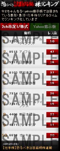
[7646]PLANT 2ch&Yahoo板統合 新着口コミ情報
※コメントは常に更新されます
Yahoo掲示板(Y板) - 7646より
967 :今日の大口の買いはな…:2025/04/30(水)18:22:00 ID:e9e*****
Yahoo掲示板(Y板) - 7646より
966 :おっ1500が見えて…:2025/04/30(水)16:20:00 ID:ユニコーン
おっ1500が見えてきましたね。
Yahoo掲示板(Y板) - 7646より
965 :何この動き?口座乗っ…:2025/04/30(水)13:38:00 ID:ユニコーン
何この動き? 口座乗っ取りでも起きたか?
【急騰】今買えばいい株22241【石破減配祭り】 より
366 :山師さん:2025/04/30(水)13:19:22 ID:oolPhORB
7646特売り
416 :山師さん:2025/04/30(水)13:26:20 hW+KDeeg
>>366
ん?乗っ取り?
Yahoo掲示板(Y板) - 7646より
964 :はい、:2025/04/30(水)13:00:00 ID:ユニコーン
はい、含み益転換 今回のトランプショックで600株だけですが買い増し致しました。
Yahoo掲示板(Y板) - 7646より
963 :今日は全く見てなかっ…:2025/04/28(月)17:47:00 ID:ユニコーン
今日は全く見てなかったけど後場は特売りスタート? でオークションも大安売り?
Yahoo掲示板(Y板) - 7646より
962 :としかして減配懸念さ…:2025/04/28(月)11:40:00 ID:ユニコーン
としかして減配懸念されてたのか?現物で安く手放した人はドンマイ。 現物最強だね
Yahoo掲示板(Y板) - 7646より
961 :無事通過:2025/04/28(月)09:43:00 ID:かまん
無事通過
Yahoo掲示板(Y板) - 7646より
960 :高配当維持だけで十分…:2025/04/25(金)21:43:00 ID:暴れん棒将軍
高配当維持だけで十分
Yahoo掲示板(Y板) - 7646より
958 :決算:2025/04/25(金)16:28:00 ID:かまん
決算
Yahoo掲示板(Y板) - 7646より
957 :まぁもう2Qの業績は…:2025/04/25(金)11:37:00 ID:ユニコーン
まぁもう2Qの業績は発表されたようなもんやし明らかな高配当株で信用買いもすくないから安心して買える希少銘柄だと思うけどな。 3年持ち続けたらまず負けはないと思う。
Yahoo掲示板(Y板) - 7646より
956 :今日寄りから張り切っ…:2025/04/24(木)15:37:00 ID:ユニコーン
今日寄りから張り切ってハイカラ入れたやつが損しただけじゃね?
Yahoo掲示板(Y板) - 7646より
955 :地元民です。:2025/04/24(木)13:47:00 ID:r30minutes-walk
地元民です。最近買い物難民が増えている。週末にPLANT行くことが楽しみだけど、車の購入維持費が月4万円くらいだから、年金だけの生活になったら行けなくなると思う。誰かに連れてってもらうか3輪の電動自転車に乗って近所のスーパーに行くかPLANT直通バスが主要駅からでるのか、PLANTも普通のスーパーみたく小さくなるのか、ある意味楽しみです。
Yahoo掲示板(Y板) - 7646より
954 :たぶんまだ下がるよ&…:2025/04/24(木)12:33:00 ID:adon
たぶんまだ下がるよ… 従業員少ないのにいろいろやらせすぎでしょ… 週末のイベントとかあれいるか? そんなことよりガラガラになった商品の補充をしっかりやった方がよいのでは… 昔はこんなことなかったんだけどな…
Yahoo掲示板(Y板) - 7646より
953 :すまない予想外した。…:2025/04/24(木)11:35:00 ID:ユニコーン
すまない予想外した。 まさかの前場プラス引け。 なぜか安売りする人いるけどオークションで最安値で売るくらいなら後場指値で売っとけよ
【急騰】今買えばいい株22208【団鬼六】 より
536 :山師さん:2025/04/21(月)22:53:54 ID:fbXSdLse
Amid Trump’s tariffs, TSMC has been stepping up its investment in the U.S. According to Economic Daily News, the company is accelerating the timeline for its second Arizona fab. In addition, TSMC is reportedly set to introduce its latest fan-out panel-level packaging (FOPLP) technology in the U.S. to meet rising demand from customers seeking chips manufactured in the U.S.
The report highlights that, following major clients such as Apple, NVIDIA, and AMD announcing plans to expand their investments in the U.S., TSMC has accordingly adjusted its strategies.
TSMC is currently in its quiet period ahead of its earnings call and is unable to comment, as the report notes.
TSMC Advances FOPLP Technology
Citing Nikkei, the report states that TSMC is finalizing the specifications for its FOPLP technology in an effort to accelerate its mass production timeline. The first-generation version is expected to adopt a 300mm x 300mm panel size—smaller than the previously tested 510mm x 515mm format. According to the report, TSMC is currently building a pilot production line in Taoyuan, Taiwan, with limited trial production anticipated to begin as early as 2027.
The report also notes that TSMC initially explored partnering with panel makers such as Innolux but ultimately opted to develop the technology in-house, as the current precision and technical capabilities of the panel industry were deemed insufficient to meet TSMC’s standards.
As noted by the report, FOPLP offers improved heat dissipation compared to 3D stacking techniques such as wafer-on-wafer (WoW), CoWoS, and SoIC. However, its production efficiency is lower than that of existing 3D stacking methods. The report adds that AI customers are still expected to be the primary adopters of this packaging technology.
Tech Giants Fuel TSMC’s U.S. Manufacturing Expansion
Notably, on April 15, AMD CEO Lisa Su confirmed that the company is ramping up U.S. production. According to Reuters, AMD’s flagship chips will soon roll off TSMC’s new Arizona line—marking the first time its products will be manufactured in the U.S.
Meanwhile, NVIDIA recently also revealed plans to invest up to USD 500 billion in U.S.-based AI server production over the next four years and confirmed that its Blackwell chips are now being produced at TSMC’s Phoenix plant, as Reuters notes.
As noted by Economic Daily News, sources indicate that in response to requests from major clients such as AMD and Apple, TSMC has reportedly informed suppliers that equipment move-in for its second Arizona fab will begin as early as September this year—one full year ahead of schedule.
In other words, the fab’s 3nm production is now expected to begin by the end of 2027, while the second-phase line for 2nm is projected to enter mass production in 2028 as the report points out.
547 :山師さん:2025/04/21(月)23:01:35 Rfp0DKa2
>>536
荒らすなボケ!
【急騰】今買えばいい株22208【団鬼六】 より
528 :山師さん:2025/04/21(月)22:51:37 ID:HQwTJw7C
Amid Trump’s tariffs, TSMC has been stepping up its investment in the U.S. According to Economic Daily News, the company is accelerating the timeline for its second Arizona fab. In addition, TSMC is reportedly set to introduce its latest fan-out panel-level packaging (FOPLP) technology in the U.S. to meet rising demand from customers seeking chips manufactured in the U.S.
The report highlights that, following major clients such as Apple, NVIDIA, and AMD announcing plans to expand their investments in the U.S., TSMC has accordingly adjusted its strategies.
TSMC is currently in its quiet period ahead of its earnings call and is unable to comment, as the report notes.
TSMC Advances FOPLP Technology
Citing Nikkei, the report states that TSMC is finalizing the specifications for its FOPLP technology in an effort to accelerate its mass production timeline. The first-generation version is expected to adopt a 300mm x 300mm panel size—smaller than the previously tested 510mm x 515mm format. According to the report, TSMC is currently building a pilot production line in Taoyuan, Taiwan, with limited trial production anticipated to begin as early as 2027.
The report also notes that TSMC initially explored partnering with panel makers such as Innolux but ultimately opted to develop the technology in-house, as the current precision and technical capabilities of the panel industry were deemed insufficient to meet TSMC’s standards.
As noted by the report, FOPLP offers improved heat dissipation compared to 3D stacking techniques such as wafer-on-wafer (WoW), CoWoS, and SoIC. However, its production efficiency is lower than that of existing 3D stacking methods. The report adds that AI customers are still expected to be the primary adopters of this packaging technology.
Tech Giants Fuel TSMC’s U.S. Manufacturing Expansion
Notably, on April 15, AMD CEO Lisa Su confirmed that the company is ramping up U.S. production. According to Reuters, AMD’s flagship chips will soon roll off TSMC’s new Arizona line—marking the first time its products will be manufactured in the U.S.
Meanwhile, NVIDIA recently also revealed plans to invest up to USD 500 billion in U.S.-based AI server production over the next four years and confirmed that its Blackwell chips are now being produced at TSMC’s Phoenix plant, as Reuters notes.
As noted by Economic Daily News, sources indicate that in response to requests from major clients such as AMD and Apple, TSMC has reportedly informed suppliers that equipment move-in for its second Arizona fab will begin as early as September this year—one full year ahead of schedule.
In other words, the fab’s 3nm production is now expected to begin by the end of 2027, while the second-phase line for 2nm is projected to enter mass production in 2028 as the report points out.
【急騰】今買えばいい株22208【団鬼六】 より
527 :山師さん:2025/04/21(月)22:51:14 ID:N5bUdpKO
Amid Trump’s tariffs, TSMC has been stepping up its investment in the U.S. According to Economic Daily News, the company is accelerating the timeline for its second Arizona fab. In addition, TSMC is reportedly set to introduce its latest fan-out panel-level packaging (FOPLP) technology in the U.S. to meet rising demand from customers seeking chips manufactured in the U.S.
The report highlights that, following major clients such as Apple, NVIDIA, and AMD announcing plans to expand their investments in the U.S., TSMC has accordingly adjusted its strategies.
TSMC is currently in its quiet period ahead of its earnings call and is unable to comment, as the report notes.
TSMC Advances FOPLP Technology
Citing Nikkei, the report states that TSMC is finalizing the specifications for its FOPLP technology in an effort to accelerate its mass production timeline. The first-generation version is expected to adopt a 300mm x 300mm panel size—smaller than the previously tested 510mm x 515mm format. According to the report, TSMC is currently building a pilot production line in Taoyuan, Taiwan, with limited trial production anticipated to begin as early as 2027.
The report also notes that TSMC initially explored partnering with panel makers such as Innolux but ultimately opted to develop the technology in-house, as the current precision and technical capabilities of the panel industry were deemed insufficient to meet TSMC’s standards.
As noted by the report, FOPLP offers improved heat dissipation compared to 3D stacking techniques such as wafer-on-wafer (WoW), CoWoS, and SoIC. However, its production efficiency is lower than that of existing 3D stacking methods. The report adds that AI customers are still expected to be the primary adopters of this packaging technology.
Tech Giants Fuel TSMC’s U.S. Manufacturing Expansion
Notably, on April 15, AMD CEO Lisa Su confirmed that the company is ramping up U.S. production. According to Reuters, AMD’s flagship chips will soon roll off TSMC’s new Arizona line—marking the first time its products will be manufactured in the U.S.
Meanwhile, NVIDIA recently also revealed plans to invest up to USD 500 billion in U.S.-based AI server production over the next four years and confirmed that its Blackwell chips are now being produced at TSMC’s Phoenix plant, as Reuters notes.
As noted by Economic Daily News, sources indicate that in response to requests from major clients such as AMD and Apple, TSMC has reportedly informed suppliers that equipment move-in for its second Arizona fab will begin as early as September this year—one full year ahead of schedule.
In other words, the fab’s 3nm production is now expected to begin by the end of 2027, while the second-phase line for 2nm is projected to enter mass production in 2028 as the report points out.
【急騰】今買えばいい株22208【団鬼六】 より
526 :山師さん:2025/04/21(月)22:51:03 ID:+p5wlGn+
Amid Trump’s tariffs, TSMC has been stepping up its investment in the U.S. According to Economic Daily News, the company is accelerating the timeline for its second Arizona fab. In addition, TSMC is reportedly set to introduce its latest fan-out panel-level packaging (FOPLP) technology in the U.S. to meet rising demand from customers seeking chips manufactured in the U.S.
The report highlights that, following major clients such as Apple, NVIDIA, and AMD announcing plans to expand their investments in the U.S., TSMC has accordingly adjusted its strategies.
TSMC is currently in its quiet period ahead of its earnings call and is unable to comment, as the report notes.
TSMC Advances FOPLP Technology
Citing Nikkei, the report states that TSMC is finalizing the specifications for its FOPLP technology in an effort to accelerate its mass production timeline. The first-generation version is expected to adopt a 300mm x 300mm panel size—smaller than the previously tested 510mm x 515mm format. According to the report, TSMC is currently building a pilot production line in Taoyuan, Taiwan, with limited trial production anticipated to begin as early as 2027.
The report also notes that TSMC initially explored partnering with panel makers such as Innolux but ultimately opted to develop the technology in-house, as the current precision and technical capabilities of the panel industry were deemed insufficient to meet TSMC’s standards.
As noted by the report, FOPLP offers improved heat dissipation compared to 3D stacking techniques such as wafer-on-wafer (WoW), CoWoS, and SoIC. However, its production efficiency is lower than that of existing 3D stacking methods. The report adds that AI customers are still expected to be the primary adopters of this packaging technology.
Tech Giants Fuel TSMC’s U.S. Manufacturing Expansion
Notably, on April 15, AMD CEO Lisa Su confirmed that the company is ramping up U.S. production. According to Reuters, AMD’s flagship chips will soon roll off TSMC’s new Arizona line—marking the first time its products will be manufactured in the U.S.
Meanwhile, NVIDIA recently also revealed plans to invest up to USD 500 billion in U.S.-based AI server production over the next four years and confirmed that its Blackwell chips are now being produced at TSMC’s Phoenix plant, as Reuters notes.
As noted by Economic Daily News, sources indicate that in response to requests from major clients such as AMD and Apple, TSMC has reportedly informed suppliers that equipment move-in for its second Arizona fab will begin as early as September this year—one full year ahead of schedule.
In other words, the fab’s 3nm production is now expected to begin by the end of 2027, while the second-phase line for 2nm is projected to enter mass production in 2028 as the report points out.
【急騰】今買えばいい株22208【団鬼六】 より
521 :山師さん:2025/04/21(月)22:50:11 ID:rwHZuuRz
Amid Trump’s tariffs, TSMC has been stepping up its investment in the U.S. According to Economic Daily News, the company is accelerating the timeline for its second Arizona fab. In addition, TSMC is reportedly set to introduce its latest fan-out panel-level packaging (FOPLP) technology in the U.S. to meet rising demand from customers seeking chips manufactured in the U.S.
The report highlights that, following major clients such as Apple, NVIDIA, and AMD announcing plans to expand their investments in the U.S., TSMC has accordingly adjusted its strategies.
TSMC is currently in its quiet period ahead of its earnings call and is unable to comment, as the report notes.
TSMC Advances FOPLP Technology
Citing Nikkei, the report states that TSMC is finalizing the specifications for its FOPLP technology in an effort to accelerate its mass production timeline. The first-generation version is expected to adopt a 300mm x 300mm panel size—smaller than the previously tested 510mm x 515mm format. According to the report, TSMC is currently building a pilot production line in Taoyuan, Taiwan, with limited trial production anticipated to begin as early as 2027.
The report also notes that TSMC initially explored partnering with panel makers such as Innolux but ultimately opted to develop the technology in-house, as the current precision and technical capabilities of the panel industry were deemed insufficient to meet TSMC’s standards.
As noted by the report, FOPLP offers improved heat dissipation compared to 3D stacking techniques such as wafer-on-wafer (WoW), CoWoS, and SoIC. However, its production efficiency is lower than that of existing 3D stacking methods. The report adds that AI customers are still expected to be the primary adopters of this packaging technology.
Tech Giants Fuel TSMC’s U.S. Manufacturing Expansion
Notably, on April 15, AMD CEO Lisa Su confirmed that the company is ramping up U.S. production. According to Reuters, AMD’s flagship chips will soon roll off TSMC’s new Arizona line—marking the first time its products will be manufactured in the U.S.
Meanwhile, NVIDIA recently also revealed plans to invest up to USD 500 billion in U.S.-based AI server production over the next four years and confirmed that its Blackwell chips are now being produced at TSMC’s Phoenix plant, as Reuters notes.
As noted by Economic Daily News, sources indicate that in response to requests from major clients such as AMD and Apple, TSMC has reportedly informed suppliers that equipment move-in for its second Arizona fab will begin as early as September this year—one full year ahead of schedule.
In other words, the fab’s 3nm production is now expected to begin by the end of 2027, while the second-phase line for 2nm is projected to enter mass production in 2028 as the report points out.
【速報】急騰・急落銘柄報告スレ18253 より
909 :山師さん@トレード中 :2025/04/15(火)15:46:26 ID:vLjn/z0F0
US chipmakers outsourcing manufacturing will escape China's tariffs(ロイター)
製造委託する米チップメーカーは中国の関税から逃れられるか
記事内
「"For all integrated circuits, whether packaged or unpackaged, the declared country of origin
for import customs purchases is the location of the wafer fabrication plant," 」
「包装されたすべての統合サーキットについては、包装されているか、梱包されていないかにかかわらず、
輸入税関の購入のために宣言された原産国は、ウェーハ製造工場の場所です。」
3日前の記事だけど、こう言う関税回避の手段って、トランプ政権内に睨まれているんだろうな (´・ω・`)
【速報】急騰・急落銘柄報告スレ18251 より
332 :山師さん@トレード中:2025/04/14(月)22:17:25 ID:rkpB0GSn0
NVIDIA Blackwell chips have started production at TSMC's chip plants in Phoenix, Arizona.
エヌビディア・ブラックウェル・チップは、アリゾナ州フェニックスにあるTSMCのチップ工場で生産を開始した。
だそうです(´・ω・`)
続きは7646銘柄情報ページでご確認ください
掲示板書き込み
- スパム対策の為、URLは"h"を抜いた"ttp"から入力して下さい。
- 宣伝目的と思われる書き込みに記載されたURLにはサイト内銘柄ページ、ブログランキング他、当サイトからのリンクを全て除外させて頂きます。
銘柄別掲示板一覧
- 【3475】 グッドコムアセット(1)
- 【9468】 KADOKAWA(1)
- 【2120】 LIFULL(1)
- 【6743】 大同信号(5)
- 【2330】 フォーサイド(1)
- 【6301】 コマツ(2)
- 【3686】 ディー・エル・イー(1)
- 【2767】 円谷フィールズホールディングス(1)
- 【3399】 丸千代山岡家(1)
- 【3133】 海帆(1)
- 【8226】 理経(5)
- 【6966】 三井ハイテック(1)
- 【9504】 中国電力(1)
- 【2764】 ひらまつ(37)
- 【9558】 ジャパニアス(1)
- 【2370】 メディネット(10)
- 【3401】 帝人(3)
- 【2418】 ツカダ・グローバルホールディング(1)
- 【2157】 コシダカホールディングス(1)
- 【3099】 三越伊勢丹ホールディングス(1)
- 【8233】 高島屋(1)
- 【6191】 エアトリ(1)
- 【7554】 幸楽苑(1)
- 【3030】 ハブ(1)
- 【3481】 三菱地所物流リート投資法人(1)
- 【3907】 シリコンスタジオ(20)
- 【3470】 マリモ地方創生リート投資法人(1)
- 【6753】 シャープ(9)
- 【2698】 キャンドゥ(1)
- 【3940】 ノムラシステムコーポレーション(1)
今日の大口の買いはなんでしょうね? 期待しかないですね!